
SI/PI Database
The SI/PI-Database is a collection of printed circuit board (PCB) based structures which represent different electromagnetic aspects for signal integrity and power integrity applications. The structures have different components and interconnecting elements e.g. vias, via-arrays, power, ground planes. Each structures contains many variations of geometry and material parameters along with the simulation results. All structures were simulated with a physics-based approach which was cross validated with a full-wave solver for different structures.
Physics-Based Approach related publications:
- Physics-Based Via and Trace Models for Efficient Link Simulation on Multilayer Structures Up to 40 GHz
- A Combined Method for Fast Analysis of Signal Propagation, Ground Noise, and Radiated Emission of Multilayer Printed Circuit Boards
- Accuracy of Physics-Based Via Models for Simulation of Dense Via Arrays
- Complete Modeling of Large Via Constellations in Multilayer Printed Circuit Boards
An overview of the structures is given in the following table along with the simulated frequency range, variations of the geometry and materials and a general description of the structure. The structure explanation has all necessary information to rebuild the setup and verify the simulation results. Additionally classification labels are explained if available.
The SI/PI-Database is intended to help the development of machine learning tools and techniques for signal integrity, power integrity and electromagnetic compatibility applications. Without the need to create the data for the machine learning investigations a performance boost during the development of the techniques should be observed.
Any usage of the data of the SI/PI-Database has to be referenced to the following article:
To get access to the data please fill out the contact form at the bottom. The download link will be provided by the entered e-mail address. You will receive an e-mail within 24 hours under normal circumstances with a download link for a zip-archive. The zip-archive contains multiple files. The description of the structure with the parameter variations is explained. A file which has all parameter variations along with classification labels and the simulation index (simu_index). The scattering parameters for the according simulation file is found by the (simu_index) . For each parameter variation with the a touchstone file simu_index.sNp is available.
Further benchmark problems related to electronic packaging are available in The Packaging Benchmark Suite by IEEE Electronics Packaging Society (EPS) Technical Committee on Electrical Design, Modeling and Simulation (TC-EDMS).
| Name | Description | No. of Simulations | Size of Compressed Data Set | Detailed Description | Image |
|---|---|---|---|---|---|
| 4-Layer Polygonal PCB based PDN | A polygonal PCb based PDN having a 4-layer stackup. In the spectrum of 1 MHz to 1 GHz 334 points are sampled. One power via (surrounded by two ground vias) are placed on the PCB having two ports. | 500 | 12 MB | 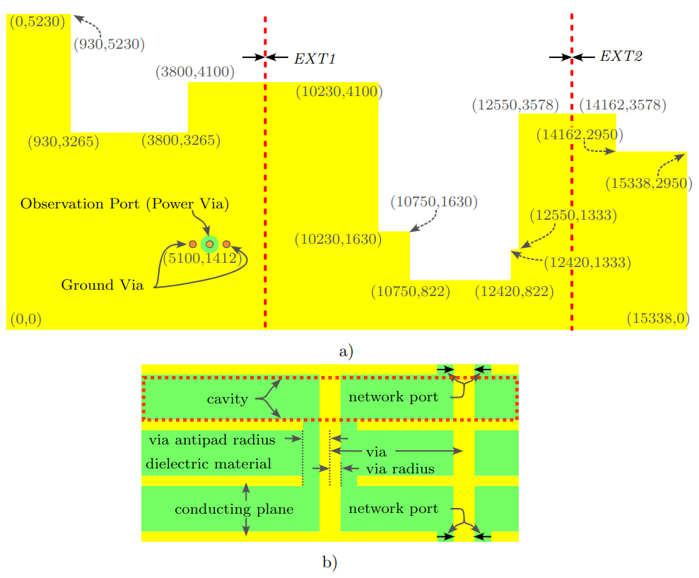 |
|
| 6-Layer PCB based PDN with two Via Arrays Latin Hypercube Sampling | A PCB setups with variations of the geometry and material are simulated with a physics-based via model. In the frequency spectrum of 1 MHz to 1 GHz 334 linear spaced frequency points are used. The PCB has two via arrays with varying positions. Overall the board has 36 ports and no components are attached. The Latin Hypercube is applied. | 985 | 7.2 GB | 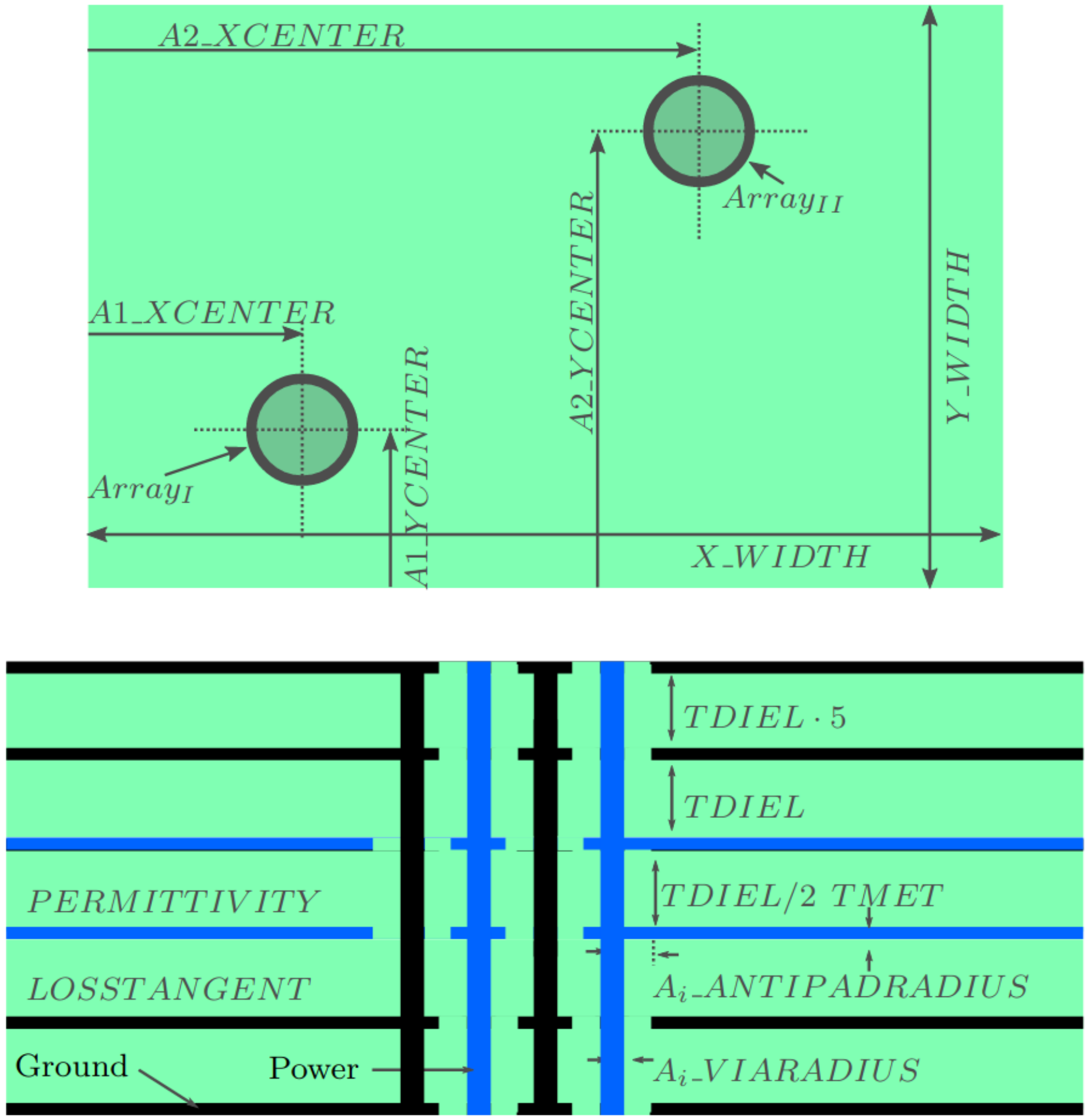 |
|
| 8-Layer PCB based PDN with two Via Arrays Latin Hypercube Sampling | A PCB setups with variations of the geometry and material are simulated with a physics-based via model. In the frequency spectrum of 1 MHz to 1 GHz 334 linear spaced frequency points are used. The PCB has two via arrays with varying positions. Overall the board has 28 ports and no components are attached. For the sampling the Latin Hypercube is applied. | 10000 | 42 GB |  |
|
| 4-Layer PCB based PDN with two Via Arrays Random Sampling | A PCB setups with variations of the geometry and material are simulated with a physics-based via model. In the frequency spectrum of 1 MHz to 1 GHz 334 linear spaced frequency points are used. The PCB has two via arrays with varying positions. Overall the board has 28 ports and no components are attached. The sampling is performed randomly. | 10000 | 44 GB |  |
|
| PWR/GND Plane PCB with 11x11 Via-Array | This structure contains a power delivery network (PDN) on a PCB with one cavity, a power plane on the bottom and a ground plane on top. One port is in the center of a via-array and is the port that is decoupled by placing decoupling capacitors (decaps) on the surrounding via array. At this port the impedance of the PDN is observed. The variations for this structure include changing the distance of the planes, the material properties and the decaps. For the decaps the location, capacitance and number was varied. The capacitors were chosen from a library containing overall 15 values including equivalent series resistance and equivalent series inductance. | 36200 | 1.3 GB |  |
|
| Link on 11 Cavity PCB with two 10x10 Via-Arrays | A link between two via-arrays was simulated. The stackup consists of 11 cavities with power and ground planes, including striplines to connect the via-arrays. 12 single ended ports are simulated. Variations are carried out for geometry and parameter. | 7031 | 2.4 GB | 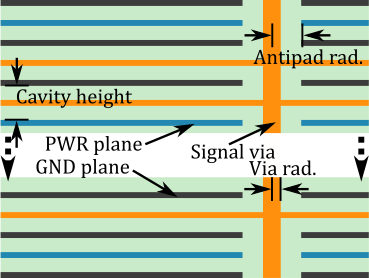 |
|
| Link on 8 Cavity PCB with two 10x10 Via-Arrays | A link between two via-arrays was simulated. The stackup consists of 8 cavities with power and ground planes, including striplines to connect the via-arrays. 12 single ended ports are simulated. Variations are carried out for geometry and parameter. | 7031 | 2.5 GB | 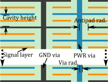 |
|
| 5x5 Via-Array on 10 Cavity PCB | A 5×5 via array is located on a 10 cavity stackup. The connection of the GND and signal vias is shown, with a via ratio of 2 : 1 for signal and GND respectively. All planes of the stackup are connected by the GND vias. All signal vias have two ports, one at the top side and on at the bottom side of the PBC. | 5000 | 12.2 GB | 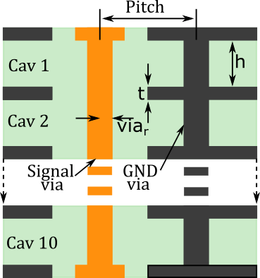 |
|
| Link on 10 Cavity PCB with two 5x5 Via-Arrays | The structure has a link between two 5x5 via-arrays. Both arrays are located on the same multilayer stackup of 10 dielectric cavities. In the fifth cavity vias of both arrays are connected by striplines. GND vias connect all planes. | 1500 | 23.7 GB | 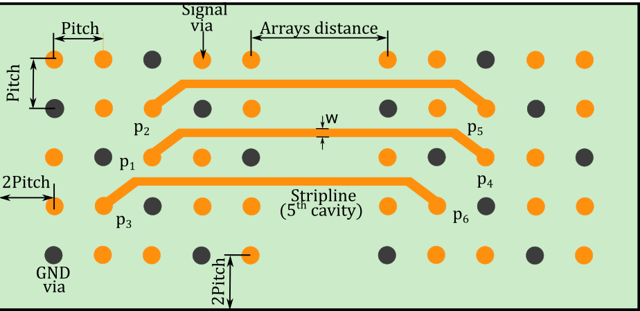 |