
Robotic Near-Field Measurement utilizing Single-Probe OTF Technique
Near-field scanning (NFS) is an important technique in evaluating the radiation and emission of electromagnetic (EM) fields originating from microwave devices and components. Over the past decades, considerable progresses have been made in enhancing scanning capabilities, including the usage of robotics, high-speed instrument communication, and high-sampling rate equipment. Despite these advancements, the time and cost of measurements are still limited by requests for large-scale, high-resolution, magnitude, and phase scanning, particularly in integrated-circuit (IC) and antenna applications concerning electromagnetic compatibility (EMC) tests.
This project aims to significantly reduce the time and cost of traditional Near-Field Scanning (NFS) by tenfold without compromising accuracy. This will be accomplished through the utilization of an innovative single-probe on-the-fly (OTF) data acquisition and processing technique. As a proof of concept, a coil antenna example has undergone testing, as depicted in (a) and (b). The technique will be extended for cost-effective indoor and outdoor EMC testing up to GHz frequencies.
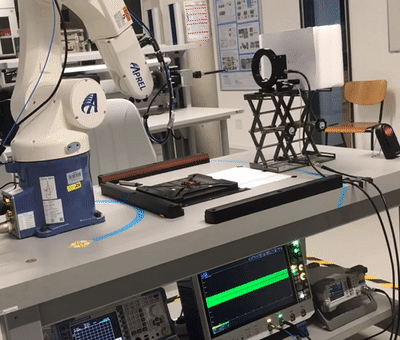
(a) NFS of a coil antenna at 125 kHz using single-probe on-the-fly, allowing a 90% reduction of time cost. (Source: TET, TUHH)

(b) Side view of two microwave probes for W-band measurements up to 110 GHz of substrate integrated waveguides on a Low Temperature Cofired Ceramic (LTCC) substrate (Source: TET, TUHH).
Contact: Dr. Cheng Yang
Related Publications:
Complex Near-Field Measurement Using On-The-Fly Scan with In-phase and Quadrature Demodulation Proceedings Article In: 15 German Microwave Conference (GeMiC), Duisburg, Germany, March 11-12, 2024. |
Single-probe Near-field Phase Retrieval using On-The-Fly Scan and Hilbert Transform Proceedings Article In: EMC Europe 2023, Krakow, Poland, September 04-08, 2023. |
Radio Frequency Measurement and Modeling of Miniaturized Components for High-Speed Applications
Dr. Yifan Qian (DAAD & CSC Fellowship) 10.07.21- 31.12.22
With increasing development of high-speed and high-integration electric and electronic systems, miniaturized components, for example, surface mounted device (SMD) capacitors, diodes, transistors and monolithic microwave integrated circuit (MMIC), are widely used in distributed radio frequency (RF) designs. As a result, accurate modeling of the impedance characteristic for miniaturized components becomes a concern in final designs.
This project co-funded by DAAD and CSC aims at developing parameterized, scalable model generation illustrated in the figure below. The key research fields are: (1) identification of major parasitic effects, (2) de-embedding/calibration techniques for both simulation and measurements, and (3) automated model synthesis.
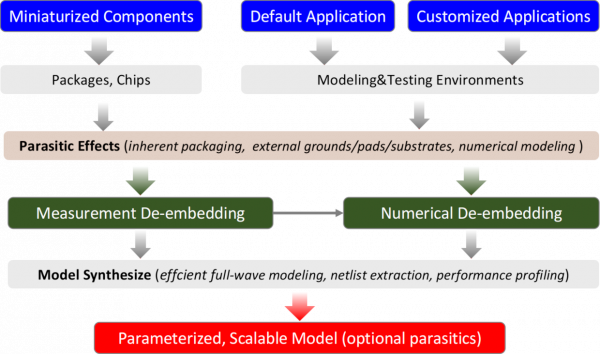
Flowchart of RF miniaturized component modeling.
A full report of his fellowship is given in the following document: PDF
Functional Via-Structures in Ceramic Multilayered Substrates
Ph.D. Thesis Ömer Faruk Yildiz. 01.01.2017 – 30.04.2021
„Low Temperature Cofired Ceramics“ (LTCC) is a technology that distinguishes itself from conventional technologies used for „Printed Circuit Boards“ (PCB) by means of a high permittivity, low dielectric losses and less manufacturing tolerances. LTCC technology is therefore especially useful for applications in microwave engineering and can allow for a high integration density of microwave devices and circuits due to the mechanical strength and high thermal conductivity of the material. To this end, via-structures (as opposed to microstrips) are supposed to be employed as functional elements for the design of filters, couplers and matching networks. That this can be an alternative to conventional methods using microstrips has already been shown and successfully applied for PCBs up to 20 GHz. This work is now to be extended to 70 GHz for use in LTCC multilayerd substrates. In doing so, established modeling techniques require to be adjusted and extended. Furthermore, appropriate testing structures will be designed as well as characterized using suitable measurement techniques.

Comparison of S-parameters of a bandpass filter implemented on a low temperature cofired ceramic (LTCC) substrate using functional vias coming from measurements and simulations. (Source: TET, TUHH).
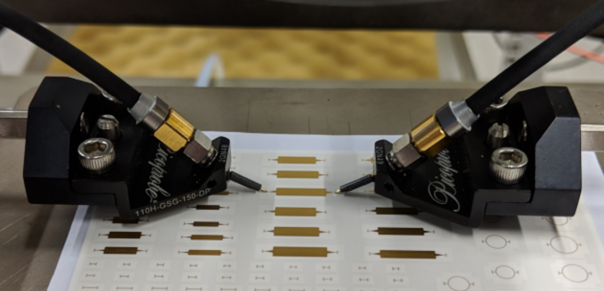
Side view of two microwave probes for W-band measurements up to 110 GHz of substrate integrated waveguides on a Low Temperature Cofired Ceramic (LTCC) substrate (Source: TET, TUHH).
Functional Via Structures in Passive Microwave Components on Multilayer Ceramic Substrates PhD Thesis 2023, ISBN: 978-3-8440-9002-4. |
Introducing Functional Via Structures to Low Temperature Cofired Ceramics: How to Optimize Reliably and Efficiently Journal Article In: IEEE Electromagnetic Compatibility Magazine, vol. 10, no. 4, pp. 35-45, 2021. |
Analysis of Differential Crosstalk and Transmission for Via Arrays in Low Temperature Cofired Ceramics Proceedings Article In: IEEE Workshop on Signal and Power Integrity (SPI), virtual event, Siegen, Germany, May 10-12, 2021. |
Vertical Integration of Passive Microwave Components Using Functional Via Structures in LTCC Multilayer Substrates Journal Article In: IEEE Transactions of Components, Packaging and Manufacturing Technology, vol. 11, no. 4, pp. 635-646, 2021. |
Vertically Integrated Microwave-Filters Using Functional Via Structures in LTCC Proceedings Article In: European Microwave Conference (EuMC), virtual event, Utrecht, Netherlands, Jan. 12-14, 2021. |
Design of Wideband Functional Via Structures for LTCC Multilayer Substrates up to 110 GHz Proceedings Article In: IEEE Electrical Design of Advanced Package & Systems Symposium (EDAPS), Kaohsiung, Taiwan, December 16-18, 2019. |
Design of Experiments for Analyzing the Efficiency of a Multi-Coil Wireless Power Transfer System Using Polynomial Chaos Expansion" Proceedings Article In: Joint International Symposium on Electromagnetic Compatibility, Sapporo, Japan, 3-7 June 2019. |
Quantifying the Impact of RF Probing Variability on TRL Calibration for LTCC Substrates Proceedings Article In: IEEE Electronic Components and Technology Conference (ECTC), Las Vegas, USA, May 28-31 2019. |
Variance-Based Iterative Model Order Reduction of Equivalent Circuits for EMC Analysis Journal Article In: IEEE Transactions on Electromagnetic Compatibility, vol. 1, pp. 128-139, 2019. |
Feasibility of Uncertainty Quantification for Power Distribution Network Modeling Using PCE and a Contour Integral Method Proceedings Article In: 2018 Joint IEEE International Symposium on Electromagnetic Compatibility & Asia-Pacific Symposium on Electromagnetic Compatibility, Singapore, May 14-17, 2018. |
Efficient Sensitivity-Aware Assessment of High-Speed Links Using PCE and Implications for COM Proceedings Article In: DesignCon, Santa Clara, CA, USA, January, 2018. |
Sensitivity Analysis and Empirical Optimization of Cross-Domain Coupling on RFICs using Polynomial Chaos Expansion Proceedings Article In: 2017 IEEE International Symposium on Electromagnetic Compatibility & Signal/Power Integrity (EMCSI) Washington, DC, USA, 2017. |
Design and Characterization of RF-Components and High-Speed Interconnects on LTCC Substrates
Industry Project, 01.12.2017 – 31.06.2019
In this project in collaboration with an industry partner various RF-components and high-speed interconnects are designed and characterized on Low Temperature Cofired Ceramics (LTCC) multilayer substrates. The project in general has the goal to gain experience in the field of multi-GHz design for both digital and analog components on LTCC. Over the course of the project, (1) LTCC substrates are analyzed by measurements and evaluated as packages for broadband communication, (2) vertical interconnects (vias) and their usage as functional elements for passive RF-components are analyzed, and (3) general design guidelines are developed based on the results obtained. Characterization is done both by simulation as well as measurement of scattering parameters up to 110 GHz.
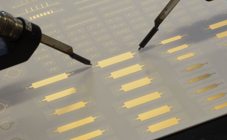
Side view of two microwave probes for broadband measurement of scattering parameters up to 50 GHz of substrate integrated waveguides on a Low Temperature Cofired Ceramic (LTCC) substrate. (Source: TET, TUHH).
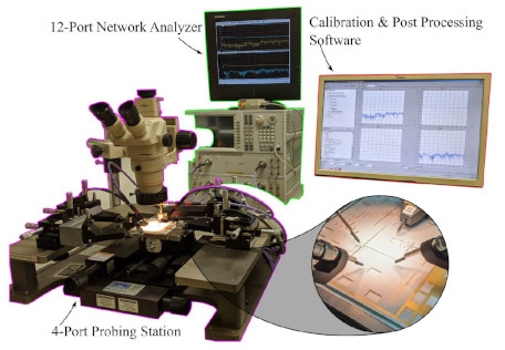
General set up of the measurement environment: Probing station holding the Low Temperature Cofired Ceramic (LTCC) substrate and providing access to it using probes, network vector analyzer for measurement of scattering parameters, and software tools for calibration and postprocessing thereof. (Source: TET, TUHH).
Design of Passive Microwave Components on Multilayered Printed Circuit Boards Using Functional Vias
Ph.D. Thesis Andreas Hardock. 01.01.2011 – 31.03.2015
This thesis deals with the design of passive microwave components such as filters, couplers and matching networks using functional vias (plated through holes) on multilayered printed circuit boards. For this purpose, the otherwise parasitic wave effects associated with vias are carefully analyzed and used functionally. The design of the components was performed on theoretical and simulation level. Scattering parameters measurements up to 35 GHz are used for validation purposes. The designs are compared to common microwave components based on microstriplines. Advantages and disadvantages with regard to electric performance and area requirements are discussed.

Multilayer subsrate simulator developed at the the Institute of Electromagnetic Theory (Source: TET, TUHH).
Top-view of a via coupler designed on a 8-layer PCB (Source: TET, TUHH).
Related Publications:
Design of Passive Microwave Components on Multilayered Printed Circuit Boards using Functional Vias PhD Thesis 2016, ISBN: 978-3-8440-4615-1. |
Modeling of Mutual Coupling between Coaxial Probes in Flat Metallic Casings Using the Contour Integral Method Proceedings Article In: 2015 International Conference on Electromagnetics in Advanced Applications (ICEAA), Turin, Italy, September 07-11, 2015. |
Physics-Based Via and Waveguide Models for Efficient SIW Simulations in Multilayer Substrates Journal Article In: IEEE Transactions on Microwave Theory and Techniques , vol. 63, no. 6, 2015. |
Efficient Calculation of External Fringing Capacitances for Physics-Based PCB Modeling Workshop 2015 IEEE 19th Workshop on Signal and Power Integrity (SPI), Berlin, Germany, May 10-13, 2015. |
Chebyshev Filter Design Using Vias as Quasi-Transmission Lines in Printed Circuit Boards Journal Article In: IEEE Transactions on Microwave Theory and Techniques, vol. 63, no. 3, 2015. |
High Frequency Measurement Techniques for Vias in Printed Circuit Boards Journal Article In: IEEE Electromagnetic Compatibility Magazine, vol. 3, no. 4, 2014. |
Using Via Stubs in Periodic Structures for Microwave Filter Design Journal Article In: IEEE Transactions on Components, Packaging and Manufacturing Technology, vol. 4, no. 7, 2014. |
Signal integrity: Efficient, physics-based via modeling: Return path, impedance, and stub effect control Journal Article In: IEEE Electromagnetic Compatibility Magazine, vol. 3, no. 1, 2014. |
Application of Vias as Functional Elements in Microwave Coupling Structures Journal Article In: IEEE Transactions on Microwave Theory and Techniques, vol. 61, no. 10, 2013. |
Analytical Extraction of Via Near-Field Coupling Using a Multiple Scattering Approach Workshop EEE Workshop on Signal and Power Integrity (SPI) Paris, Frankreich, 2013. |
Minimizing Displacement Return Currents in Multilayer Via Structures Proceedings Article In: IEEE Conference on Electrical Performance of Electronic Packaging and Systems (EPEPS), Tempe, USA, October 21-24, 2012. |
Double Stub Matching in Multilayered Printed Circuit Board using Vias Proceedings Article In: Electronic Components and Technology Conference (ECTC), San Diego, USA, May 29-June 1, 2012. |
Probing and Fixturing Techniques for Wideband Multiport Measurements in Digital Packaging
Ph. D. Thesis Miroslav Kotzev. 01.10.2007 – 29.02.2013
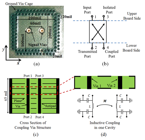
This thesis deals with test signal probing and fixturing techniques for wideband multiport measurements in digital packaging in the frequency range from a few MHz to 50 GHz. Three different signal launch techniques are investigated in time and frequency domains. At first, the performance of the coaxial surface mounted connector launch is explored in case of crosstalk measurements in a backplane connector via pin field. In the next step the recessed probe launche technique is briefly presented. After that the main focus is on the results obtained in recent investigations with respect to the launch calibration, application to measurements of embedded mulitlayer structures and modifications to improve the launch bandwidth. Finally, the concept of a novel multiport probing fixture is presented and its electrical performance explored. Using a simple two-tier calibration procedure, the effect of the probing fixture on measurements of dense via array structures is reduced and the results obtained are validated with microprobe based measurements. Based on 3D full-wave electromagnetic modeling, suggestions for layout optimization are made which will be needed to extend the applicability of these techniques to data rates of 20 Gbit/s and beyond.
TUHH Universitätsbibliothek. TUBDok Link: http://doku.b.tu-harburg.de/volltexte/2013/1210/
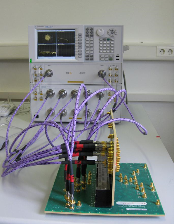
12-port vector network analyzer from Agilent Technologies connected to backplane connector test vehicle (courtesy of IBM Development Böblingen,Germany)(Source: TET, TUHH).
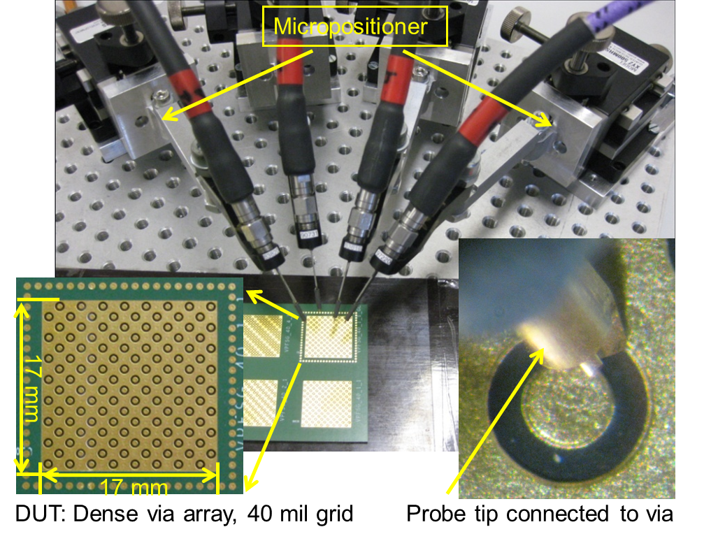
Multiport probing measurement setup for investigations in dense via structures applying commercial microprobes and micropositioners (Source: TET, TUHH).
Related Publications:
Probing and Fixturing Techniques for Wideband Multiport Measurements in Digital Packaging PhD Thesis 2013, ISBN: 978-3-8440-1910-0. |
Electrical Performance of the Recessed Probe Launch Technique for Measurement of Embedded Multilayer Structures Journal Article In: IEEE Transactions on Instrumentation and Measurement, vol. 61, no. 12, 2012. |
Electrical Performance of a Multiport Interposer for Measurements of Dense Via Arrays Workshop IEEE Workshop on Signal Propagation on Interconnects (SPI), Naples, Italy, May 8-11, 2011. |
Custom-Made Calibration Standards for Measurements of Multilayer Substrates Proceedings Article In: German Microwave Conference (GeMic), Darmstadt, Germany, March 14-16, 2011. |
Effect of Via Stubs on the TRL Calibration Technique for Measurement of Embedded Multilayer Structures Proceedings Article In: European Microwave Conference (EuMC), Paris, France, September 28-30, 2010. |
Crosstalk Analysis in High Density Connector Via Pin Fields for Digital Backplane Applications Using a 12-Port Vector Network Analyzer Proceedings Article In: IEEE Conference of Electronics System Integration Technology (ESTC), Berlin, Germany, September 13-16, 2010. |
Multiport Measurement and Deembedding Techniques for Crosstalk Study in Via Arrays Workshop IEEE Workshop on Signal Propagation on Interconnects (SPI), Hildesheim, Germany, May 9-12, 2010. |
Extraction of Broadband Error Boxes for Microprobes and Recessed Probe Launches for Measurement of Printed Circuit Board Structures Proceedings Article In: IEEE Workshop on Signal Propagation on Interconnects (SPI), Strasbourg, France, May 12-15, 2009. |
Bandwidth Study of Recessed Probe Launch Variations for Broadband Measurement of Embedded PCB Structures Proceedings Article In: German Microwave Conference (GeMic), Munich, Germany, March 16-18, 2009. |