
Development of an Automated Storage of Numerical Simulation Results Based on OpenBIS
Tommy Weber, Research Assistant, 01.06.2023-30.11.2023
Storage and documentation of simulation data is fundamental. Therefore, an automated storage system for simulation data is wanted in combination with a database. The first phase of the project combines two systems:
- Storage system (E.g. OpenBIS, https://openbis.ch/), incl. data storage, versioning, and SQL database
- Providing interface to internal simulation tools of the TET institute (https://www.tet.tuhh.de/en/concept-2/), by a python wrapper. Primary focus is on CONMLS. However, the possibility to connect other tools is to be considered e.g. CONCEPT-II, CONMTL.
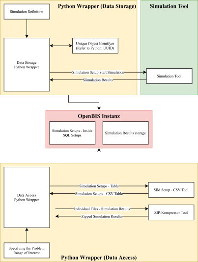
The first phase has an environment as result which enables to define experiments. An experiment can be e.g. a printed circuit board (PCB) (layers, ports, vias, …). Within the experiment simulations are performed with respect to variations of specified parameters (e.g. geometry of the PCB). Data points are sampled based on a random, latin hypercube, or active sampling. Simulation results are stored as scattering parameters on the storage system. Simulation results and setups can be retrieved fully from the storage system. At the end of phase one the functionality should be provided for internal use in the institute of electromagnetic theory.
High Speed Automotive Interconnect Design for Gbps Links
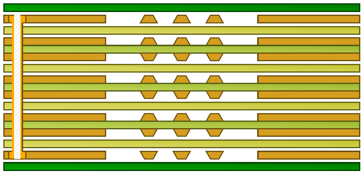
High-speed interconnect design for wired links in digital systems has been a well-established field of research and innovation for several decades now. In contrast, automotive high-speed interconnects have only recently advanced to higher and higher data rates. Correspondingly, models for components specific to automotive interconnects have not been created or validated to a large extent nor has a sufficient model-to-hardware correlation been established. In addition, automotive high-speed interconnects must fulfill strict requirements regarding electromagnetic compatibility (EMC) regulations. This project aims to develop high-speed interconnect models used in automotive applications on a system level. These models will be adapted to analyze printed circuit board (PCBs) stack-ups used in automotive applications in combination with assembly and interconnection technologies (AITs) and provide insight of the Signal Integrity performance of high-speed links in harsh automotive environmental standards to have a functional system which fulfill the electrical performance as well as reliability requirements.
Multilayered PCB Stack-Up used in an Automatve Application.

Extracted Insertion Loss of a Transmission Line using a Delta-L Deembedding Algorithm. Conductor Loss and Dielectric Loss are extracted via the Curve-Fitted Insertion Loss of the DUT.
Funding: Robert Bosch GmbH
Contact: Jose Enrique Hernandez Bonilla
Start date: 01.09.2022
Data-Driven Design and Analysis of High-Speed Interconnects on PCBs
The expansion of information networks such as the Industrial Internet of Things (IoT) is creating an ever-increasing demand for data. As a logical consequence, this creates a demand for data generation, processing, storage and data transport between these steps. This project is investigating ways of ensuring fast data transport. The aim is to use machine learning (ML) methods to accelerate the design process for high-speed connections. The main focus is on the structure of the PCB, but the effects of line coding and equalizers are also considered. The overall aim is to create a large SI/PI database on the basis of which a hybrid design flow can be created that combines data-driven and physics-based methods. It will be investigated for which sub-areas and in which way the respective ML methods can be used optimally.
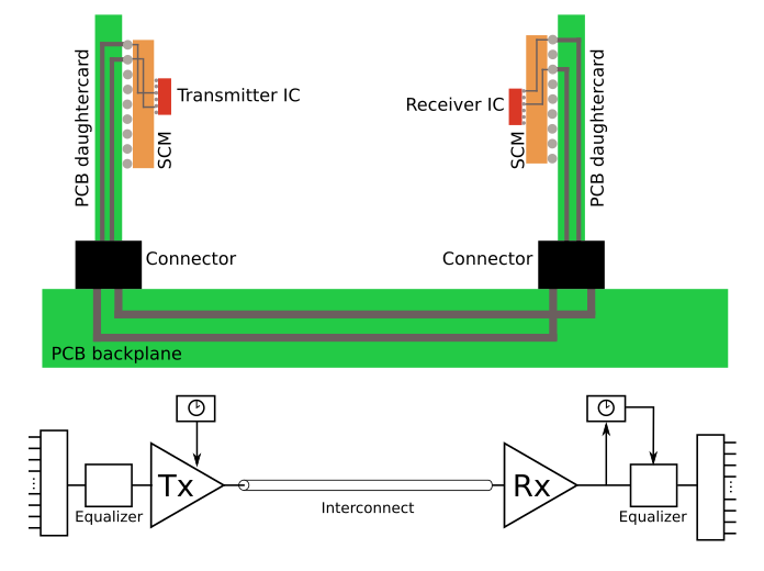
Schematic drawing of a connection between two microchips across a backplane.
Physics-based simulation of a generic differential link in a multi-layer PCB structure.
Funding: Freie und Hansestadt Hamburg
Contact: Til Hillebrecht, M.Sc.
Start date: 17.10.2022
Electronic Design Flow Improvement with Machine Learning Tools
The design of modern printed circuit boards (PCBs) is a challenging task and requires the compliance with a variety of specifications. To reduce the risk of a poor design and getting the desired functionality, the design processs is accompanied by many electromagnetic simulations. In combination with the time requirement of an individual simulaion this results in a large effort which needs a lot of computational resources. Because future designs will have a higher complexity and larger integration level, decreasing the time requirement for an individual simulation is an important task to solve. Without improving the simulation mechanism the design ow will require more time which results in additional costs for the development. This project aims to improve the design ow by providing a more efficient design tool and process. In the area of machine learning algorithms some promising ideas are found. Publications in recent years provide methods to increase the efficiency of optimization processes – for example generic algorithms for the placement of decoupling capacitors. With artificial neural networks first results are achieved by investigating the impedance of the power delivery network under the in uence of decoupling capacitors. Future work shall increase the applicability of artificial neural networks to a wider range of simulation tasks. Therefore different aspects have to be investigated. The focus is on printed circuit boards which are commonly used in many electronic devices. The functionality and capabilities of printed circuit boards is well understood. One of the most important aspects within this project is to provide not only a faster simulation ow but to ensure the consistency of simulation results with existing tools and methods.

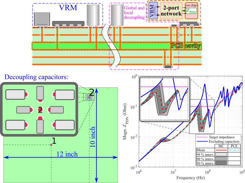
Typical multilayer printed circuit board with four layers. Two layers are for the power supply and two layers are for the signal transmission. By placing decoupling capacitors on the PCB the impedance of the power delivery network shall be improved. Multiple parameters (material constants and dimensions) are influencing
the eletrical behavior of the PCB.

The target impedance is violated by the impedance of the power delivery network, thereby the design is not sufficient. This fact can either be taken from a conventional simulations tool or with an artificial neural network. Using artificial neural networks is a promising idea. Depending on different input parameters (material constants and dimensions) predictions of the electrical behavior are made.
Funding: Freie und Hansestadt Hamburg
Contact: Morten Schierholz, M.Sc.
Start date: 01.10.2021
Application of Model Order Reduction Techniques to the Simulation of Complex Interconnect Systems
Interconnects in modern electronic systems constitute very dense and complex structures that demand highly efficient methodologies for their modeling and design. Even with semi-analytical or hybrid simulation approaches, the analysis of this type of systems often implies very large models and long execution times. This project, which is developed in collaboration with the Instituto Tecnológico de Costa Rica (ITCR), deals with the exploration of numerical techniques to facilitate the handling and processing of such complex models.
Different macromodeling techniques, such as vector fitting algorithms and matrix state representations, are being explored as an additional resource that can assist the handling, concatenation, and processing of interconnect models. Stochastic frequency-domain macromodels, combining the descriptor form representation for a dynamical system with the Polynomial Chaos Expansion technique, are also being analyzed. This will allow to include the variability analysis of the system for any frequency over a desired frequency range. To reduce the number of required samples, techniques for the analytical concatenation of macromodels in descriptor form will be adapted. Together with the use of semi-analytical techniques for the sample construction, this process should guarantee the accurate representation of complex multiport systems with different random input variables, within a short time. To evaluate the performance of these techniques, the comparison with purely numerical techniques will be addressed with realistic modeling scenarios.

Example of a Vector fitting approximation of an S-Parameter crosstalk model as a function of the number of poles.
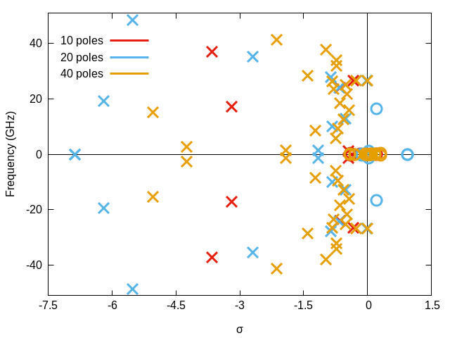
Complex plane pole and zero constellation of a vector fitting (VF) macromodel as a function of the number of poles, extracted from a high-speed channel S-Parameter model.
Funding: Instituto Tecnologico de Costa Rica (ITCR)
Contact: Luis Ernesto Carrera Retana, M. Sc., Prof. Renato Rimolo-Donadio
Start date: 01.01.2017
Related Publications:
Construction of Reciprocal Macromodels in the Loewner Matrix Framework Journal Article In: IEEE Transactions on Microwave Theory and Techniques, vol. 71, no. 8, pp. 3561-3571, 2023. |
Improving Accuracy After Stability Enforcement in the Loewner Matrix Framework Journal Article In: IEEE Transaction on Microwave Theory and Techniques, vol. 70, no. 2, pp.1037-1047, 2022. |
Efficient Construction of Interconnect Passive Macromodels Through Segmented Analysis Proceedings Article In: IEEE Conference on Electrical Performance of Electronic Packaging and Systems (EPEPS), San Jose, CA, USA, Oct. 14-17, 2018. |
Evaluation of Concatenation Techniques for State-Space Interconnect Macromodels”, IEEE Conference on Electrical Performance of Electronic Packaging and Systems (EPEPS) Proceedings Article In: IEEE Conference on Electrical Performance of Electronic Packaging and Systems (EPEPS), San Jose, CA, USA, Oct. 15-18, 2017. |
Evaluation of Vector Fitting for Compact Interconnect Model Representation Proceedings Article In: IEEE Convention of Central America and Panama Region (CONCAPAN) San Jose, Costa Rica, 2016. |
Evaluation of Interconnects up to 100 GHz Using Machine Learning
Ph. D. Thesis Katharina Scharff: 16.04.2016 – 15.10.2020
This thesis presents a contribution to the evaluation and modeling of high-speed electrical interconnects on printed circuit boards up to 100 GHz using machine learning. Parametric studies of different models are conducted with efficient numerical methods. The crosstalk is analyzed for different interconnect types. Machine learning methods are introduced as an alternative design method. They are evaluated regarding the reliability of the predictions and the necessary effort.
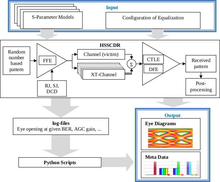
Data flow and concurrence of tools used in this study. Random jitter (RJ), sinusoidal jitter (SJ), as well as duty cycle distortion (DCD) are added as part of the transmitter as indicated. Furthermore, a voltage swing of 1V and a slew rate of 44 ps applies. (Source: TET, TUHH).
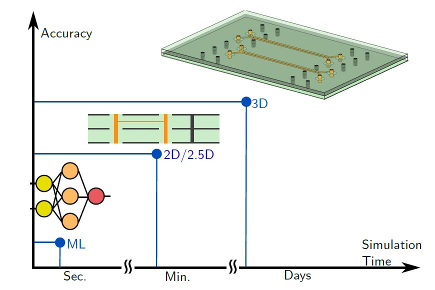
Tools bases on Machine Learning (ML) often show very short simulation times when compared to physics based tools for signal integrity applications – be them 2D/2.5D or fully 3D. They fall behind though in accuracy and flexibility. It all depends therefore on a smart usage of ML. (Source: TET, TUHH).
Related Publications:
Bayesian Optimization of First-Order Continuous-Time Linear Equalization in High-Speed Links Including Crosstalk Proceedings Article In: IEEE Workshop on Signal and Power Integrity (SPI), Aveiro, Portugal, May 07-10, 2023. |
Evaluation of Interconnects up to 100 GHz Using Machine Learning PhD Thesis 2022, ISBN: 978-3-8440-8534-1. |
ANN Performance for the Prediction of High-Speed Digital Interconnects over Multiple PCBs Proceedings Article In: IEEE Conference on Electrical Performance of Electronic Packaging and Systems (EPEPS) San Jose, CA, USA, 2020. |
Bayesian Optimization for Signal Transmission Including Crosstalk in a Via Array Proceedings Article In: International Symposium on Electromagnetic Compatibility, Rome, Italy, Sept. 23-25, 2020. |
Evaluation of Neural Networks to Predict Target Impedance Violations of Power Delivery Networks Proceedings Article In: IEEE Conference on Electrical Perfomance of Electronic Packaging and Systems (EPEPS) Montreal, Canada, October 6-9, 2019. |
Mode Conversion Due To Residual Via Stubs in Differential Signaling Proceedings Article In: IEEE Workshop on Signal and Power Integrity (SPI) Chambery, France, June 18-21, 2019. |
Via Transition Optimization Using a Domain Decomposition Approach Proceedings Article In: IEEE Workshop on Signal and Power Integrity (SPI), Chambery, France, June 18-21 2019. |
Performance Metrics for Crosstalk on Printed Circuit Boards in Frequency Domain Proceedings Article In: IEEE Workshop on Signal and Power Integrity (SPI), Chambéry, France, June 18-21 2019. |
Efficient Crosstalk Analysis of Differential Links on Printed Circuit Boards Up to 100 GHz Journal Article In: IEEE Transactions on Electromagnetic Compatibility, vol. 61, no. 6, pp. 1849-1859, February 26, 2019. |
Physical Scaling Effects of Differential Crosstalk in Via Arrays up to Frequencies of 100 GHz Proceedings Article In: IEEE Workshop on Signal and Power Integrity (SPI), Brest, France, May 22 -25, 2018. |
Efficient Prediction of Equalization Effort and Channel Performance for PCB-Based Data Links Journal Article In: IEEE Transactions on Components, Packaging and Manufacturing Technology, vol. 7, no. 11, 2017. |
Exploration of Differential Via Stub Effect Mitigation by Using PAM4 and PAM8 Line Coding Proceedings Article In: IEEE Workshop on Signal and Power Integrity (SPI), Lake Maggiore (Baveno), Italy, May 7-10, 2017. |
Exploring Efficient Variability-Aware Analysis Method for High-Speed Digital Link Design Using PCE Proceedings Article In: UBM DesignCon Conference, Santa Clara, CA, USA, January 31 – February 2, 2017. |
Variability Analysis of via Crosstalk using Polynomial Chaos Expansion Proceedings Article In: UBM DesignCon Conference, Santa Clara, CA, USA, January 31-February 2, 2017. |
Impact of Continuous Time Linear Equalizer Variability on Eye Opening of High-Speed Links Proceedings Article In: IEEE Workshop on Signal and Power Integrity (SPI), Turin, Italy, May 8-11, 2016. |
Stochastic Contour Integral Methodology for the Computation of Two-Dimensional Electromagnetic Wave Propagation
David Dahl, DFG Project 01.08.2015 – 31.07.2018
The project will extend the so-called contour integral method (CIM) for the computation of two-dimensional packaging and interconnect structures such as printed circuit boards and planar optical substrates to take into account stochastic boundary conditions and simulation parameters. The stochastic contour integral method will be studied from a mathematical point of view, implemented in a numerically efficient way, and demonstrated with relevant application examples. To take into account stochastic boundary conditions and input parameters, the polynomial chaos expansion (PCE) known from other application areas will for the first time be applied in the context of a contour integral method for electrodynamics. For this purpose, a partially existing Fortran code will be extended by methods that can take into account statistical variations in the excitation as well as in the geometry and material parameters of the structure under investigation. On the one hand, a mathematical analysis of the stochastic contour integral methodology will be carried out, including demonstrations of the methodology with help of suitable examples and investigations with regard to the limitations of the numerical treatment. On the other hand, the methodology and the existing numerical code will be extended specifically for stochastic problems in the areas of microwave engineering and integrated planar optics. The potential of the methodology will be demonstrated by applying the extended code to structures that are relevant from an engineering point of view. By virtue of the cooperation between the Institute of Electromagnetic Theory and the Institute of Mathematics of the Hamburg University of Technology (TUHH) the project will facilitate fundamental research in mathematics and numerics in the context of a relevant and challenging application area in engineering.
The contour integral methods can be applied for the modeling of power distribution networks in printed circuit boards. The PCE can be used to study the influence of variations of the decoupling capacitor properties. (Source: TET, TUHH).
The contour integral method can be applied in planar optics for the efficient simulation of photonic crystals which can be used for building optical waveguides. (Source: TET, TUHH).
Related Publications:
Efficient Simulation of Substrate-Integrated Waveguide Antennas Using a Hybrid Boundary Element Method Journal Article In: IEEE Journal on Multiscale and Multiphysics Computational Techniques, vol. 4, pp. 180-189, 2019. |
Prediction of Frequency Dependent Shielding Behavior for Ground Via Fences in Printed Circuit Boards Proceedings Article In: IEEE Workshop on Signal and Power Integrity (SPI), Chambery, France, June 18-21, 2019. |
Quantifying the Impact of RF Probing Variability on TRL Calibration for LTCC Substrates Proceedings Article In: IEEE Electronic Components and Technology Conference (ECTC), Las Vegas, USA, May 28-31 2019. |
Multiscale Simulation of 2D Photonic Crystal Structures Using a Contour Integral Method Journal Article In: IEEE Journal on Multiscale and Multiphysics Computational Techniques, vol. 4, pp. 88-97, 2019. |
An Intrusive PCE Extension of the Contour Integral Method and its Application in Electrical Engineering Proceedings Article In: Annual Meeting of the Gesellschaft für Angewandte Mathematik und Mechanik (GAMM), Vienna, Austria, February, 2019. |
Novel method for error estimation in applications of polynomial chaos expansion to stochastic modeling of multi-resonant systems Proceedings Article In: IEEE Conference on Electrical Performance of Electronic Packaging and Systems (EPEPS), San Jose, CA, USA, Oct. 14-17, 2018. |
Error Estimation in Applications of Polynomial Chaos Expansion to Stochastic Modeling of multi-Resonant Systems Proceedings Article In: IEEE Conference on Electrical Perfomance of Electronic Packaging and Systems (EPEPS), San Jose, USA, Oct. 14-17, 2018. |
Electromagnetic Modeling and Optimization of Through Silicon Vias PhD Thesis 2018, ISBN: 978-3-8440-6009-6. |
Physical Scaling Effects of Differential Crosstalk in Via Arrays up to Frequencies of 100 GHz Proceedings Article In: IEEE Workshop on Signal and Power Integrity (SPI), Brest, France, May 22 -25, 2018. |
Feasibility of Uncertainty Quantification for Power Distribution Network Modeling Using PCE and a Contour Integral Method Proceedings Article In: 2018 Joint IEEE International Symposium on Electromagnetic Compatibility & Asia-Pacific Symposium on Electromagnetic Compatibility, Singapore, May 14-17, 2018. |
Effect of 3D Stack-Up Integration on Through Silicon Via Characteristics Proceedings Article In: IEEE Workshop on Signal and Power Integrity (SPI), Lake Maggiore (Baveno), Italy, May 7-10, 2017. |
Efficient Total Crosstalk Analysis of Large Via Arrays in Silicon Interposers Journal Article In: IEEE Transactions on Components, Packaging and Manufacturing Technology, vol. 6, no. 12, 2016. |
Modeling of Differential Striplines in Segmented Simulation of Printed Circuit Board Link Proceedings Article In: IEEE Signal and Power Integrity Conference (SIPI 2016), Ottawa, ON, Canada, July 25-29, 2016. |
High Frequency Characterization of Silicon Substrate and through Silicon Vias Proceedings Article In: Electronic Components and Technology Conference (ECTC), Las Vegas, US, May 31 – June 3, 2016. |
On the Upper Bound of Total Uncorrelated Crosstalk in Large Through Silicon Via Arrays Proceedings Article In: IEEE Workshop on Signal and Power Integrity (SPI) Turin, Italy, May 8-11, 2016. |
A Rigorous Approach for the Rigorous Approach Using Multipole Expansions Journal Article In: IEEE Transactions on Components, Packaging and Manufacturing Technology, vol. 6, no. 1, 2016. |
Efficient Computation of Localized Fields for Through Silicon Via Modeling Up to 500 GHz Journal Article In: IEEE Transactions on Components, Packaging and Manufacturing Technology, vol. 5, no. 12, 2015. |
Comparison of Passivation Materials for High frequency 3D Packaging Application up to 110 GHz Proceedings Article In: 2015 European Microelectronics Packaging Conference (EMPC), Friedrichshafen, Germany, September 14-16, 2015. |
Efficient Calculation of External Fringing Capacitances for Physics-Based PCB Modeling Workshop 2015 IEEE 19th Workshop on Signal and Power Integrity (SPI), Berlin, Germany, May 10-13, 2015. |
2015 IEEE 19th Workshop on Signal and Power Integrity (SPI), Berlin, Germany, May 10-13, 2015. |
Effect of Layered Media on the Parallel Plate Impedance of Printed Circuit Boards Proceedings Article In: EEE Electrical Design of Advanced Packaging and Systems (EDAPS) Symposium, Bangalore, India, December 14-16, 2014. |
Analysis of Wave Propagation along Coaxial Through Silicon Vias Using a Matrix Method Workshop IEEE Workshop on Signal and Power Integrity (SPI), Ghent, Belgium, May 11-14, 2014. |
Applying a physics-based via model for the simulation of Through Silicon Vias Proceedings Article In: IEEE Conference on Electrical Performance of Electronic Packaging and Systems (EPEPS), San Jose, USA, October 27-30, 2013. |
IEEE Workshop on Signal and Power Integrity (SPI), Paris, France, May-12-15, 2013. |
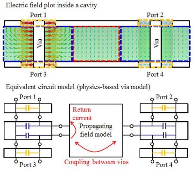
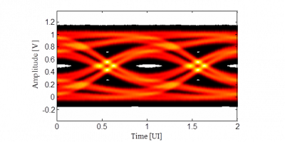
Combined Assessment of Interconnect and Equalization in Data Links on Multilayer Printed Circuit Boards
Ph. D. Thesis Torsten Reuschel. 01.10.2013 – 15.10.2018
Increasing data rates and reduced design margins oppose a detailed consideration of the diverse aspects of high-speed digital links, such as the passive channel, equalization, and coding. This work offers novel methods for the computationally efficient design and validation of links. A combined system perspective is established based on predominant physical parameters of the interconnect and key parameters of equalizer design. This enables a systematic prediction of design constraints and is accompanied by a study of advanced uncertainty quantification methods for pre- and post-layout design.
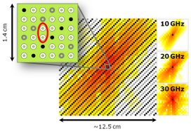
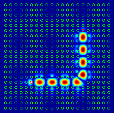
Crosstalk distribution in large via-array at different frequencies. The simulation is carried out using the tool Multilayer Substrate Simulator, which is developed at the institute. (Source: TET, TUHH).
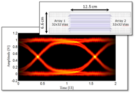
Exemplary interconnect between two large via-arrays. The striplines within the first cavity are indicated. The eye diagram is efficiently generated using statistical methods. (Source: TET, TUHH).
Related Publications:
Automated Generation and Correlation of Physics-Based Via Models with Full-Wave Simulation for an SI/PI Database Proceedings Article In: Conference on Electrical Performance of Electronic Packaging and Systems (EPEPS), Milpitas, CA, USA, October 15-18, 2023. |
Modeling Electrically Long Interconnects Using Physics-Informed Delayed Gaussian Processes Journal Article In: IEEE Transactions on Electromagnetic Compatibility, vol. 65, no. 6, pp. 1715 - 1723, 2023. |
Modeling S-parameters of Interconnects using Periodic Gaussian Process Kernels Proceedings Article In: IEEE Workshop on Signal and Power Integrity (SPI), Aveiro, Portugal, May 07-10, 2023. |
Combined Assessment of Interconnect and Equalization in Data Links on Multilayer Printed Circuit Boards PhD Thesis 2019, ISBN: 978-3-8440-6499-5. |
Direct Prediction of Linear Equalization Coefficients Using Raised Cosine Pulse Shaping in Frequency Domain Proceedings Article In: IEEE Workshop on Signal and Power Integrity (SPI), Brest, France, May 22-25, 2018. |
Efficient Sensitivity-Aware Assessment of High-Speed Links Using PCE and Implications for COM Proceedings Article In: DesignCon, Santa Clara, CA, USA, January, 2018. |
Efficient Prediction of Equalization Effort and Channel Performance for PCB-Based Data Links Journal Article In: IEEE Transactions on Components, Packaging and Manufacturing Technology, vol. 7, no. 11, 2017. |
Efficient Design of Continuous Time Linear Equalization for Loss Dominated Digital Links Proceedings Article In: IEEE Workshop on Signal and Power Integrity (SPI), Lake Maggiore (Baveno), Italy, May 7-10, 2017. |
Exploration of Differential Via Stub Effect Mitigation by Using PAM4 and PAM8 Line Coding Proceedings Article In: IEEE Workshop on Signal and Power Integrity (SPI), Lake Maggiore (Baveno), Italy, May 7-10, 2017. |
An Electronically Scannable Reflector Antenna Using a Planar Active Array Feed at Ka-Band Journal Article In: IEEE Transactions on Microwave Theory and Techniques, vol. 65, no. 5, 2017. |
Redundant and Non-Redundant Spectrum Shaping Schemes for Reflection-Limited Chip-to-Chip Communication Proceedings Article In: International ITG Conference on Systems, Communication and Coding (SCC) Hamburg, Germany, February 6-9, 2017. |
Variability Analysis of via Crosstalk using Polynomial Chaos Expansion Proceedings Article In: UBM DesignCon Conference, Santa Clara, CA, USA, January 31-February 2, 2017. |
Exploring Efficient Variability-Aware Analysis Method for High-Speed Digital Link Design Using PCE Proceedings Article In: UBM DesignCon Conference, Santa Clara, CA, USA, January 31 – February 2, 2017. |
Efficient Total Crosstalk Analysis of Large Via Arrays in Silicon Interposers Journal Article In: IEEE Transactions on Components, Packaging and Manufacturing Technology, vol. 6, no. 12, 2016. |
Ansatz zur Verbesserung des Vorstellungsvermögens elektromagnetischer Felder der Studierenden im Modul „Theoretische Elektrotechnik I: Zeitunabhängige Felder“ Journal Article In: Praxisprojekte des Qualifizierungsprogramms „Forschendes Lernen an der TUHH“, Ausgabe 2. Hamburg, Germany: Zentrum für Lehre und Lernen, Technische Universität Hamburg, 2016. |
On the Treatment of Arbitrary Boundary Conditions Using a Fast Direct H-Matrix Solver in MoM Journal Article In: IEEE Transactions on Antennas and Propagation, vol. 64, no. 8, 2016. |
Modeling of Differential Striplines in Segmented Simulation of Printed Circuit Board Link Proceedings Article In: IEEE Signal and Power Integrity Conference (SIPI 2016), Ottawa, ON, Canada, July 25-29, 2016. |
On the Upper Bound of Total Uncorrelated Crosstalk in Large Through Silicon Via Arrays Proceedings Article In: IEEE Workshop on Signal and Power Integrity (SPI) Turin, Italy, May 8-11, 2016. |
Impact of Continuous Time Linear Equalizer Variability on Eye Opening of High-Speed Links Proceedings Article In: IEEE Workshop on Signal and Power Integrity (SPI), Turin, Italy, May 8-11, 2016. |
Segmented Physics-Based Modeling of Multilayer Printed Circuit Boards Using Stripline Port Journal Article In: IEEE Transactions on Electromagnetic Compatibility, vol. 58, no. 1, 2016. |
Systematic analysis of electrical link bottlenecks and strategies for their equalization Proceedings Article In: DesignCon, Santa Clara, CA, USA, 19. -21. January , 2016. |
Energy-Aware Signal Integrity Analysis for High-Speed PCB Links Journal Article In: IEEE Transactions on Electromagnetic Compatibility, vol. 57, no. 5, 2015. |
Investigation of Long Range Differential Crosstalk on Printed Circuit Boards Workshop EEE Workshop on Signal and Power Integrity (SPI), Ghent, Belgium, May 11-14, 2014. |
Electromagnetic Modeling and Optimization of Through Silicon Vias
Ph. D. Thesis David Dahl. 01.10.2012 – 13.12.2017
This thesis presents the simulation and the design of vertical interconnects in silicon substrates known as through silicon vias (TSVs) which are applied as a component of 3D integration of integrated circuits. Numerical methods of comparably high efficiency are developed and applied in order to simulate the electromagnetic properties of large realistic arrays of TSVS. The proposed methods are correlated with alternative methods and parameter variations are carried out to derive design guidelines. Further, several test structures with TSV are developed and the measurement results are correlated with the results from electromagnetic simulations.
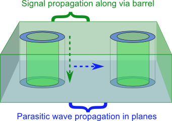
Schematic layout of a part of a silicon interposer where Through Silicon Vias (TSV) establish a connection between top and bottom of the structure. The metallic barrels of typically circular cross-section are electrically isolated from the conductive silicon substrate material by a thin silicon dioxide layer. Two principle types of wave propagation are investigated. (Source: TET, TUHH).
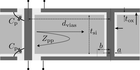
A physics-based via model assuming metallic boundaries on top and bottom of the interposer structure. The near field effects are modeled by lumped capacitances while wave propagation in the cavity constituted by the substrate and the enclosing metallic layers is represented by the “parallel plate impedance”. (Source: TET, TUHH).
Related Publications:
Efficient Simulation of Substrate-Integrated Waveguide Antennas Using a Hybrid Boundary Element Method Journal Article In: IEEE Journal on Multiscale and Multiphysics Computational Techniques, vol. 4, pp. 180-189, 2019. |
Prediction of Frequency Dependent Shielding Behavior for Ground Via Fences in Printed Circuit Boards Proceedings Article In: IEEE Workshop on Signal and Power Integrity (SPI), Chambery, France, June 18-21, 2019. |
Quantifying the Impact of RF Probing Variability on TRL Calibration for LTCC Substrates Proceedings Article In: IEEE Electronic Components and Technology Conference (ECTC), Las Vegas, USA, May 28-31 2019. |
Multiscale Simulation of 2D Photonic Crystal Structures Using a Contour Integral Method Journal Article In: IEEE Journal on Multiscale and Multiphysics Computational Techniques, vol. 4, pp. 88-97, 2019. |
An Intrusive PCE Extension of the Contour Integral Method and its Application in Electrical Engineering Proceedings Article In: Annual Meeting of the Gesellschaft für Angewandte Mathematik und Mechanik (GAMM), Vienna, Austria, February, 2019. |
Novel method for error estimation in applications of polynomial chaos expansion to stochastic modeling of multi-resonant systems Proceedings Article In: IEEE Conference on Electrical Performance of Electronic Packaging and Systems (EPEPS), San Jose, CA, USA, Oct. 14-17, 2018. |
Error Estimation in Applications of Polynomial Chaos Expansion to Stochastic Modeling of multi-Resonant Systems Proceedings Article In: IEEE Conference on Electrical Perfomance of Electronic Packaging and Systems (EPEPS), San Jose, USA, Oct. 14-17, 2018. |
Electromagnetic Modeling and Optimization of Through Silicon Vias PhD Thesis 2018, ISBN: 978-3-8440-6009-6. |
Physical Scaling Effects of Differential Crosstalk in Via Arrays up to Frequencies of 100 GHz Proceedings Article In: IEEE Workshop on Signal and Power Integrity (SPI), Brest, France, May 22 -25, 2018. |
Feasibility of Uncertainty Quantification for Power Distribution Network Modeling Using PCE and a Contour Integral Method Proceedings Article In: 2018 Joint IEEE International Symposium on Electromagnetic Compatibility & Asia-Pacific Symposium on Electromagnetic Compatibility, Singapore, May 14-17, 2018. |
Effect of 3D Stack-Up Integration on Through Silicon Via Characteristics Proceedings Article In: IEEE Workshop on Signal and Power Integrity (SPI), Lake Maggiore (Baveno), Italy, May 7-10, 2017. |
Efficient Total Crosstalk Analysis of Large Via Arrays in Silicon Interposers Journal Article In: IEEE Transactions on Components, Packaging and Manufacturing Technology, vol. 6, no. 12, 2016. |
Modeling of Differential Striplines in Segmented Simulation of Printed Circuit Board Link Proceedings Article In: IEEE Signal and Power Integrity Conference (SIPI 2016), Ottawa, ON, Canada, July 25-29, 2016. |
High Frequency Characterization of Silicon Substrate and through Silicon Vias Proceedings Article In: Electronic Components and Technology Conference (ECTC), Las Vegas, US, May 31 – June 3, 2016. |
On the Upper Bound of Total Uncorrelated Crosstalk in Large Through Silicon Via Arrays Proceedings Article In: IEEE Workshop on Signal and Power Integrity (SPI) Turin, Italy, May 8-11, 2016. |
A Rigorous Approach for the Rigorous Approach Using Multipole Expansions Journal Article In: IEEE Transactions on Components, Packaging and Manufacturing Technology, vol. 6, no. 1, 2016. |
Efficient Computation of Localized Fields for Through Silicon Via Modeling Up to 500 GHz Journal Article In: IEEE Transactions on Components, Packaging and Manufacturing Technology, vol. 5, no. 12, 2015. |
Comparison of Passivation Materials for High frequency 3D Packaging Application up to 110 GHz Proceedings Article In: 2015 European Microelectronics Packaging Conference (EMPC), Friedrichshafen, Germany, September 14-16, 2015. |
Efficient Calculation of External Fringing Capacitances for Physics-Based PCB Modeling Workshop 2015 IEEE 19th Workshop on Signal and Power Integrity (SPI), Berlin, Germany, May 10-13, 2015. |
2015 IEEE 19th Workshop on Signal and Power Integrity (SPI), Berlin, Germany, May 10-13, 2015. |
Effect of Layered Media on the Parallel Plate Impedance of Printed Circuit Boards Proceedings Article In: EEE Electrical Design of Advanced Packaging and Systems (EDAPS) Symposium, Bangalore, India, December 14-16, 2014. |
Analysis of Wave Propagation along Coaxial Through Silicon Vias Using a Matrix Method Workshop IEEE Workshop on Signal and Power Integrity (SPI), Ghent, Belgium, May 11-14, 2014. |
Applying a physics-based via model for the simulation of Through Silicon Vias Proceedings Article In: IEEE Conference on Electrical Performance of Electronic Packaging and Systems (EPEPS), San Jose, USA, October 27-30, 2013. |
IEEE Workshop on Signal and Power Integrity (SPI), Paris, France, May-12-15, 2013. |
Software-Benchmarking for Signal and Power Integrity Applications
Industry Project. 01.03.2012 – 31.12.2014
The Institute of Electromagnetic Theory is evaluating SPEAG’s SEMCAD software, a FDTD based field solver, with respect to typical problems in signal and power integrity design of digital systems. Schmid & Partner Engineering AG (SPEAG) is a Zurich based company that develops and manufactures advanced numerical tools and instrumentation for evaluation of electromagnetic near- and far-fields from static to optical frequencies. SPEAG focuses on evaluation and optimization of EM fields in complex environments such as close to and within the human body. Typical applications include EM safety and design optimization of mobile phones, MRI, and medical implants.
Below is a benchmark from electronic packaging: A ball grid array (BGA) socket model consisting of approx. 28 million cells. Reflection, transmission, and crosstalk parameters were extracted in the frequency domain up to 40 GHz from time domain data. It can be seen that the crosstalk reaches a maximum in the frequency range from 10 to 15 GHz.

SEMCAD model of ball grid array socket.

S-parameters obtained from SEMCAD simulations.
A second benchmark is the silicon interposer below with a pair of through silicon vias (TSVs) consisting of about 1 million cells. Results from time domain simulation using two digital pulses for excitation are shown. It can be seen that the TSVs shows mostly inductive reflection and produce crosstalk during rise and fall times.
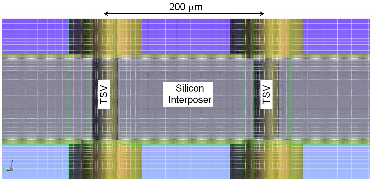
SEMCAD model of silicon interposer with through silicon vias.
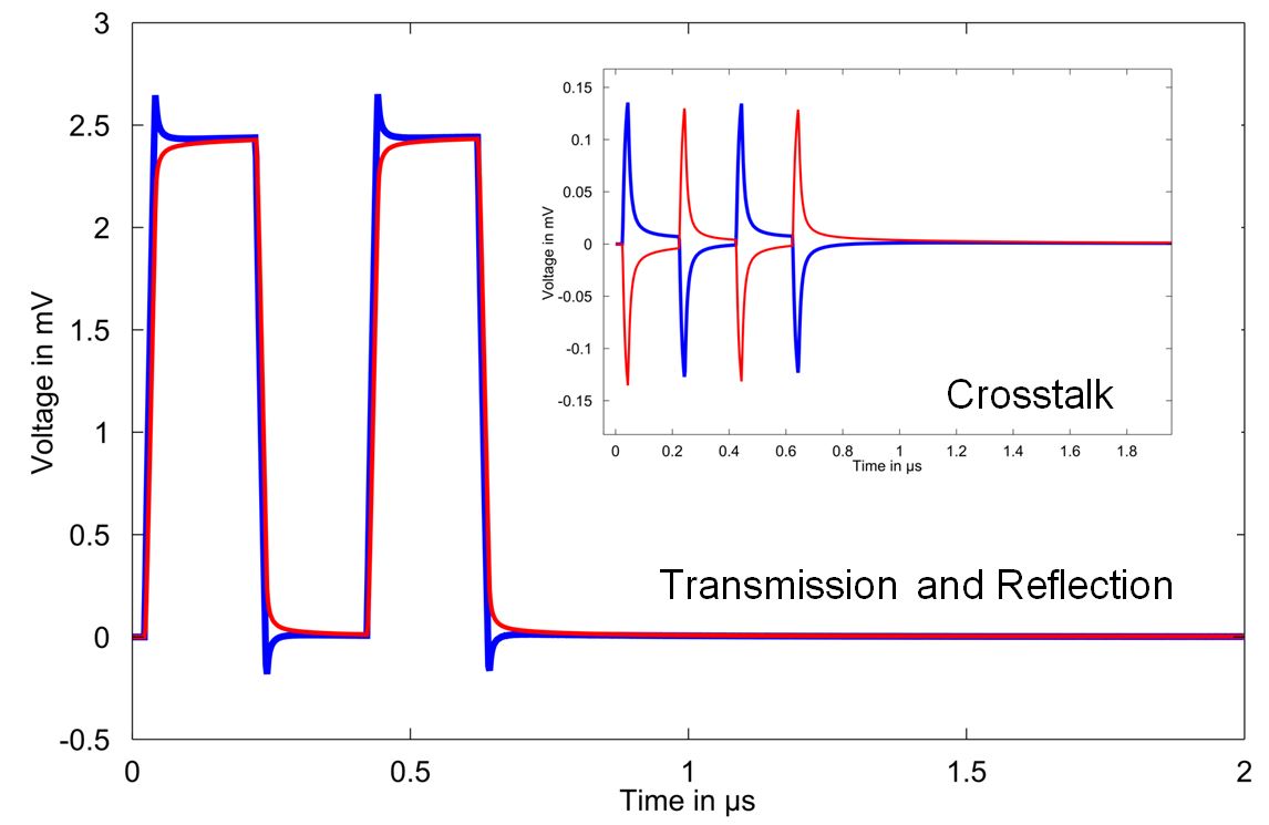
Time domain results from SEMACD simulation.
50+ Gbps High Speed Serial Link Design for Digital Systems
Industry Project. 01.08.2014 – 31.10.2014
High speed serial link design for digital systems is rapidly approaching the 25-50 Gbps data rate and is likely to move beyond in the next decade as can be seen e.g. from the recent 56 Gbps Common Electrical Interface (CEI) initiative of the Optical Internetworking Forum (OIF). With the increase in data rate problems in the areas of signal integrity (SI), power integrity (PI), and electromagnetic compatibility (EMC) will exacerbate and require more attention than before in order to achieve a system that is not threatened in its electrical integrity (see figure below).
In this research project the Institute of Electromagnetic Theory was investigating on behalf of HUAWEI Research Europe the state of the art, the technical issues, and the necessary steps for electrical integrity at such advanced data rates. Specifically the following research areas were addressed in detail
– basic elements of successful link design methodologies,
– necessary CAD tools for link design,
– specific problems and challenges at 50+ Gbps signaling,
– suitable packaging & interconnect structures for 50+ Gbps signaling,
– most important research areas in the near future.
The results were summarized in a White Paper and presented at HUAWEI.

The concept of electrical integrity for digital systems: Typically, three aspects of electrical integrity are distinguished (left): power integrity, signal integrity, and electromagnetic compatibility. Although the three aspects have different objectives and use different methodologies, they are closely interlinked. The schematic at the right side of the figure illustrates the target domains of the different aspects, which can roughly be described as follows: Power integrity is concerned with providing a noise free power supply, signal integrity is concerned with the quality of signal transmission, and the electromagnetic compatibility is concerned with mitigating electromagnetic interference.
Via Array Modeling for Application in Fast, Energy-Efficient Digital Systems
Ph. D. Thesis Sebastian Müller. 01.04.2010 – 31.07.2014
This thesis studies the application of physics-based via models for an efficient modeling of large via arrays in multiglayer PCBs. Three main aspects are addressed: the study and improvement of the modeling accuray, the study and improvement of the model efficiency, and the application of the model in a systematic evaluation of via array design alternatives for high speed links.
With regard to the modeling accuracy, the application of an improved local field model is identified as a suitable way to improve the model accuraxy for the simulation of via arrays, especially at frequencies above 20 GHz. With the improved model, an accurate simulation of via arrays with a pitch of 60 mil or larger becomes possible in the frequency range up to 50 GHz. Improvements with regard to the model efficiency lead to a reduction of calculation times which allows to carry out fast design explorations for smaller via arrays on a stadard PC. Finally, an approach for the systematic design ebaluation is presented which intefrates the adventages of the efficient physics-based via model in a larger concept. With the approach, a quantitative comparison of design alternatives bevomes possible that takes into account the impact of design changes on both signal integrity and energy efficiency for the complete system.
(Source: TET, TUHH).
(Source: TET, TUHH).
Related Publications:
Segmented Physics-Based Modeling of Multilayer Printed Circuit Boards Using Stripline Port Journal Article In: IEEE Transactions on Electromagnetic Compatibility, vol. 58, no. 1, 2016. |
Energy-Aware Signal Integrity Analysis for High-Speed PCB Links Journal Article In: IEEE Transactions on Electromagnetic Compatibility, vol. 57, no. 5, 2015. |
Effect of Layered Media on the Parallel Plate Impedance of Printed Circuit Boards Proceedings Article In: EEE Electrical Design of Advanced Packaging and Systems (EDAPS) Symposium, Bangalore, India, December 14-16, 2014. |
Including multiconductor transmission lines in a quasi-analytical model for multilayer structures PhD Thesis 2014, ISBN: 978-3-8440-3360-1. |
High Frequency Measurement Techniques for Vias in Printed Circuit Boards Journal Article In: IEEE Electromagnetic Compatibility Magazine, vol. 3, no. 4, 2014. |
Investigation of Long Range Differential Crosstalk on Printed Circuit Boards Workshop EEE Workshop on Signal and Power Integrity (SPI), Ghent, Belgium, May 11-14, 2014. |
Energy-aware analysis of electrically long high speed I/O links Journal Article In: Computer Science – Research and Development, vol. 29, no. 2, 2014. |
Einfluss der Routinglage in Via-Arrays auf die Signalqualität bei hohen Datenraten Proceedings Article In: Internationale Fachmesse und Kongress für Elektromagnetische Verträglichkeit (EMV Düsseldorf) , Düsseldorf, Germany, March 11-13, 2014. |
Signal integrity: Efficient, physics-based via modeling: Return path, impedance, and stub effect control Journal Article In: IEEE Electromagnetic Compatibility Magazine, vol. 3, no. 1, 2014. |
Analytical Extraction of Via Near-Field Coupling Using a Multiple Scattering Approach Workshop EEE Workshop on Signal and Power Integrity (SPI) Paris, Frankreich, 2013. |
Complete Modeling of Large Via Constellations in Multilayer Printed Circuit Boards Journal Article In: IEEE Transactions on Components, Packaging and Manufacturing Technology, vol. 3, no. 3, 2013. |
Signal and Power Integrity (SPI) Co-Analysis for High-Speed Communication Channels Proceedings Article In: UBM DesignCon Conference, Santa Clara, USA, January 28-31, 2013. |
Minimizing Displacement Return Currents in Multilayer Via Structures Proceedings Article In: IEEE Conference on Electrical Performance of Electronic Packaging and Systems (EPEPS), Tempe, USA, October 21-24, 2012. |
Accuracy of Physics-Based Via Models for Simulation of Dense Via Arrays Journal Article In: IEEE Transactions on Electromagnetic Compatibility, vol. 54, no. 5, 2012. |
Energy-Aware Analysis of Electrically Long High Speed I/O Links Journal Article In: Computer Science – Research and Development, August 2012 and International Conference on Energy-Aware High Performance Computing (EnA-HPC), Hamburg, Germany, September 12, 2012. |
Efficient, Physics-Based Via Modeling: Integration of Striplines (invited) Journal Article In: IEEE Electromagnetic Compatibility Magazine, vol. 1, no. 2, 2012. |
Analytical Calculation of Conduction and Displacement Current Contributions in PCB Return Current Paths Proceedings Article In: Asia-Pacific EMC Symposium (APEMC), Singapore, May 21-24, 2012. |
Anwendung quasianalytischer Via-Modelle zur schnellen Simulation dichter Via-Arrays Proceedings Article In: Internationale Fachmesse und Kongress für Elektromagnetische Verträglichkeit (EMV Düsseldorf), Düsseldorf, Germany, February 7-9, 2012. |
Backplane Channel Design Optimization: Recasting a 3Gb/s Link to Operate at 25Gb/s and Above Proceedings Article In: UBM DesignCon Conference, Santa Clara, CA, USA, January 30-February 2, 2012. |
Impact of Multiple Scattering on Passivity of Equivalent-Circuit Via Models Proceedings Article In: IEEE Electrical Design of Advanced Package & Systems Symposium (EDAPS), Hangzhou, China, December 12-14, 2011. |
Recent Developments of Via and Return Current Path Modeling (Invited) Proceedings Article In: International Conference on Electromagnetics in Advanced Applications (ICEAA), Torino, Italy, September 12-16, 2011. |
Validation and Application of Physics-based Via Models to Dense Via Arrays Proceedings Article In: IEC DesignCon Conference, Santa Clara, USA, January 31-February 3, 2011. |
Non-Uniform Currents on Vias and Their Effects in a Parallel-Plate Environment Proceedings Article In: IEEE Electrical Design of Advanced Package & Systems Symposium (EDAPS), Singapore, December 7-9, 2010. |
Effect of Mixed-Reference Planes on Single-Ended and Differential Links in Multilayer Substrates Workshop IEEE Workshop on Signal Propagation on Interconnects (SPI), Hildesheim, Germany, May 9-12, 2010. |
Schnelle Simulation verlustbehafteter Verbindungsstrukturen auf Leiterplatten auf der Grundlage quasianalytischer Via-Modelle und der Leitungstheorie Proceedings Article In: Internationale Fachmesse und Kongress für Elektromagnetische Verträglichkeit (EMV Düsseldorf), Düsseldorf, Germany, March 9-11, 2010. |
Exploration of Power Supply Noise Effects on Maximum Data Rates of High Speed Digital Links in Advanced Server Systems
Industry Project. 18.06.2010 – 17.06.2013
High speed digital links in IBM’s server systems today are running at data rates of up to 10 Gigabit per second (Gbps). These links are crucial for the overall performance of the system and are carefully designed with respect to signal integrity and bit error rates. The design process follows an iterative procedure in which I/O circuit designers and package designers collectively optimize the link performance using appropriate models for each element of the communication system. As data rates increase in next generation platforms to exceed 12 Gbps, the fundamental noise coupling mechanisms will change making a localized nearest neighbour analysis less relevant. Newer architectures are also increasingly relying on differential links to provide a measure of noise rejection. Increasing data rates will involve new noise coupling mechanisms, many of which are increasingly sensitive to skew, power supply noise, and return current path discontinuities.

IBM Watson Supercomputer based on Power7 (Source: IBM)
Transistors on IBM Power6 Chip (Source: IBM)
The design process for high speed digital links is nowadays focused on the assessment of signal interconnect performance. Power delivery network design is usually a separate effort and its implications for signal quality and maximum achievable data rates are not routinely studied or accurately quantified. In this joint research project the Institute of Electromagnetic Theory in close collaboration with a team from IBM Germany Research & Development explored the effect of power supply noise on the maximum achievable data rates in IBM’s high speed digital links. The team developed successfully a power delivery model for packaging structures and a method for inclusion of simultaneous switching noise into the link budget simulation.

Simulated eye diagram for a high speed digital link.
Simulated eye diagram subject to power supply noise.
Related Publications:
Modeling of Power Supply Noise Effects on High Speed Interconnects Workshop EMC Symposium (APEMC), Melbourne, Australia, Mai 20-23, 2013. |
Signal and Power Integrity (SPI) Co-Analysis for High-Speed Communication Channels Proceedings Article In: UBM DesignCon Conference, Santa Clara, USA, January 28-31, 2013. |
Framework for Co-Simulation of Signal and Power Integrity in Server Systems Proceedings Article In: IEEE Conference on Electrical Performance of Electronic Packaging and Systems (EPEPS), Tempe, USA, October 21-24, 2012. |
IEEE Workshop on Signal and Power Integrity (SPI), Sorrento, Italy, May 13-16, 2012. |
Development, Validation and Application of Semi-Analytical Interconnect Models for Efficient Simulation of Multilayer Substrates
Ph. D. Thesis Renato Rimolo-Donadio. 01.11.2006 – 31.12.2010
This project deals with the efficient modeling and simulation of multilayer substrates in high-speed electronic systems.
Semi-analytical models for vias and traces in packages and printed circuit boards are proposed and incorporated into a framework for automatic simulation of multilayer structures. The models are validated with general-purpose numerical methods for electromagnetic simulation and measurements, using typical configurations such as differential and single-ended links. Application scenarios of realistic complexity for signal integrity, power integrity, and electromagnetic compatibility are evaluated and the co-simulation of these three domains is explored.
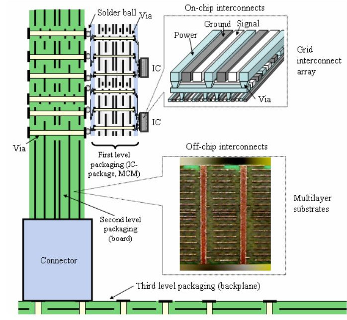
Illustration of interconnect levels in high-speed electronic systems. On-chip interconnects mainly consist of metallization layers of IC technologies, which are typically arranged as grid meshes. Off-chip interconnects cover the first (package and MCM), second (board), and third (motherboard/backplane) levels. Multilayer substrates are used to support the off-chip signal and power networks. (Source: TET, TUHH).

Functional block diagram of the modeling approach for simulation of multilayer substrates. The figure depicts the interrelation between the different model components. (Quelle: TET, TUHH).
Related Publications:
FNNs Models for Regression of S-Parameters in Multilayer Interconnects with Different Electrical Lengths Proceedings Article In: 2023 IEEE MTT-S Latin America Microwave Conference (LAMC), San José, Costa Rica, December 06-08, 2023. |
Construction of Reciprocal Macromodels in the Loewner Matrix Framework Journal Article In: IEEE Transactions on Microwave Theory and Techniques, vol. 71, no. 8, pp. 3561-3571, 2023. |
Improving Accuracy After Stability Enforcement in the Loewner Matrix Framework Journal Article In: IEEE Transaction on Microwave Theory and Techniques, vol. 70, no. 2, pp.1037-1047, 2022. |
ANN Hyperparameter Optimization by Genetic Algorithms for Via Interconnect Classification Proceedings Article In: IEEE Workshop on Signal and Power Integrity (SPI), virtual event, Siegen, Germany, May 10-12, 2021. |
SI/PI-Database of PCB-Based Interconnects for Machine Learning Applications Journal Article In: IEEE Access, vol. 9, pp. 34423-34432, 2021. |
Via Transition Optimization Using a Domain Decomposition Approach Proceedings Article In: IEEE Workshop on Signal and Power Integrity (SPI), Chambery, France, June 18-21 2019. |
Mode Conversion Due To Residual Via Stubs in Differential Signaling Proceedings Article In: IEEE Workshop on Signal and Power Integrity (SPI) Chambery, France, June 18-21, 2019. |
Efficient Construction of Interconnect Passive Macromodels Through Segmented Analysis Proceedings Article In: IEEE Conference on Electrical Performance of Electronic Packaging and Systems (EPEPS), San Jose, CA, USA, Oct. 14-17, 2018. |
Evaluation of Concatenation Techniques for State-Space Interconnect Macromodels”, IEEE Conference on Electrical Performance of Electronic Packaging and Systems (EPEPS) Proceedings Article In: IEEE Conference on Electrical Performance of Electronic Packaging and Systems (EPEPS), San Jose, CA, USA, Oct. 15-18, 2017. |
Efficient Prediction of Equalization Effort and Channel Performance for PCB-Based Data Links Journal Article In: IEEE Transactions on Components, Packaging and Manufacturing Technology, vol. 7, no. 11, 2017. |
Evaluation of Vector Fitting for Compact Interconnect Model Representation Proceedings Article In: IEEE Convention of Central America and Panama Region (CONCAPAN) San Jose, Costa Rica, 2016. |
Systematic analysis of electrical link bottlenecks and strategies for their equalization Proceedings Article In: DesignCon, Santa Clara, CA, USA, 19. -21. January , 2016. |
Energy-Aware Signal Integrity Analysis for High-Speed PCB Links Journal Article In: IEEE Transactions on Electromagnetic Compatibility, vol. 57, no. 5, 2015. |
High Frequency Measurement Techniques for Vias in Printed Circuit Boards Journal Article In: IEEE Electromagnetic Compatibility Magazine, vol. 3, no. 4, 2014. |
Using Via Stubs in Periodic Structures for Microwave Filter Design Journal Article In: IEEE Transactions on Components, Packaging and Manufacturing Technology, vol. 4, no. 7, 2014. |
Signal integrity: Efficient, physics-based via modeling: Return path, impedance, and stub effect control Journal Article In: IEEE Electromagnetic Compatibility Magazine, vol. 3, no. 1, 2014. |
Application of Vias as Functional Elements in Microwave Coupling Structures Journal Article In: IEEE Transactions on Microwave Theory and Techniques, vol. 61, no. 10, 2013. |
Analytical Extraction of Via Near-Field Coupling Using a Multiple Scattering Approach Workshop EEE Workshop on Signal and Power Integrity (SPI) Paris, Frankreich, 2013. |
Complete Modeling of Large Via Constellations in Multilayer Printed Circuit Boards Journal Article In: IEEE Transactions on Components, Packaging and Manufacturing Technology, vol. 3, no. 3, 2013. |
Electrical Performance of the Recessed Probe Launch Technique for Measurement of Embedded Multilayer Structures Journal Article In: IEEE Transactions on Instrumentation and Measurement, vol. 61, no. 12, 2012. |
Accuracy of Physics-Based Via Models for Simulation of Dense Via Arrays Journal Article In: IEEE Transactions on Electromagnetic Compatibility, vol. 54, no. 5, 2012. |
Efficient, Physics-Based Via Modeling: Integration of Striplines (invited) Journal Article In: IEEE Electromagnetic Compatibility Magazine, vol. 1, no. 2, 2012. |
Circular Ports in Parallel-Plate Waveguide Analysis with Isotropic Excitations Journal Article In: IEEE Transactions on Electromagnetic Compatibility, vol. 54, no. 3, 2012. |
Double Stub Matching in Multilayered Printed Circuit Board using Vias Proceedings Article In: Electronic Components and Technology Conference (ECTC), San Diego, USA, May 29-June 1, 2012. |
Analytical Calculation of Conduction and Displacement Current Contributions in PCB Return Current Paths Proceedings Article In: Asia-Pacific EMC Symposium (APEMC), Singapore, May 21-24, 2012. |
Analysis and Mitigation of Parasitic Mode Conversion for Microstrip to Stripline Transitions Journal Article In: IEEE Transactions on Electromagnetic Compatibility, vol. 54, no. 2, 2012. |
Anwendung quasianalytischer Via-Modelle zur schnellen Simulation dichter Via-Arrays Proceedings Article In: Internationale Fachmesse und Kongress für Elektromagnetische Verträglichkeit (EMV Düsseldorf), Düsseldorf, Germany, February 7-9, 2012. |
Extension of the Contour Integral Method to Anisotropic Modes on Circular Ports Journal Article In: IEEE Transactions on Components, Packaging and Manufacturing Technology, vol. 2, no. 2, 2012. |
Backplane Channel Design Optimization: Recasting a 3Gb/s Link to Operate at 25Gb/s and Above Proceedings Article In: UBM DesignCon Conference, Santa Clara, CA, USA, January 30-February 2, 2012. |
Impact of Multiple Scattering on Passivity of Equivalent-Circuit Via Models Proceedings Article In: IEEE Electrical Design of Advanced Package & Systems Symposium (EDAPS), Hangzhou, China, December 12-14, 2011. |
Recent Developments of Via and Return Current Path Modeling (Invited) Proceedings Article In: International Conference on Electromagnetics in Advanced Applications (ICEAA), Torino, Italy, September 12-16, 2011. |
A Hybrid CIM/MoM Approach for Power Plane Analysis Including Radiation Loss Proceedings Article In: Asia-Pacific EMC Symposium (APEMC), Jeju Island, Korea, May-16-19, 2011. |
Fast Parametric Pre-Layout Analysis of Signal Integrity for Backplane Interconnects Proceedings Article In: IEEE Workshop on Signal Propagation on Interconnects (SPI), Naples, Italy, May 8-11, 2011. |
Validation and Application of Physics-based Via Models to Dense Via Arrays Proceedings Article In: IEC DesignCon Conference, Santa Clara, USA, January 31-February 3, 2011. |
Development, Validation, and Application of Semi-analytical Interconnect Models for Efficient Simulation of Multilayer Substrates PhD Thesis 2011, ISBN: 978-3-8325-2776-1 . |
Non-Uniform Currents on Vias and Their Effects in a Parallel-Plate Environment Proceedings Article In: IEEE Electrical Design of Advanced Package & Systems Symposium (EDAPS), Singapore, December 7-9, 2010. |
Effect of Mixed-Reference Planes on Single-Ended and Differential Links in Multilayer Substrates Workshop IEEE Workshop on Signal Propagation on Interconnects (SPI), Hildesheim, Germany, May 9-12, 2010. |
Multiport Measurement and Deembedding Techniques for Crosstalk Study in Via Arrays Workshop IEEE Workshop on Signal Propagation on Interconnects (SPI), Hildesheim, Germany, May 9-12, 2010. |
A Combined Method for Fast Analysis of Signal Propagation, Ground Noise, and Radiated Emission of Multilayer Printed Circuit Boards Journal Article In: IEEE Transactions on Electromagnetic Compatibility , vol. 52, no. 2, 2010. |
Fast and Concurrent Simulations for SI, PI, and EMI Analysis of Multilayer Printed Circuit Boards (invited) Proceedings Article In: Asia-Pacific Symposium on EMC (APEMC), Beijing, China, April 12-16, 2010. |
Schnelle Simulation verlustbehafteter Verbindungsstrukturen auf Leiterplatten auf der Grundlage quasianalytischer Via-Modelle und der Leitungstheorie Proceedings Article In: Internationale Fachmesse und Kongress für Elektromagnetische Verträglichkeit (EMV Düsseldorf), Düsseldorf, Germany, March 9-11, 2010. |
Fast-Physics-Based Via and Trace Models for Signal and Power Integrity Co-Analysis Proceedings Article In: IEC DesignCon Conference, Santa Clara, USA, February 1-4, 2010. |
Special Session on Power Integrity Techniques: Contour Integral Method for Rapid Computation of Power/Ground Plane Impedance Proceedings Article In: IEC DesignCon Conference, Santa Clara, USA, February 1-4, 2010. |
Comprehensive Multilayer Substrate Models for Co-Simulation of Power and Signal Integrity Proceedings Article In: IMAPS 42th International Symposium on Microelectronics and Packaging, San Jose, California, USA, November 3-5, 2009. |
Hybrid Approach for Efficient Calculation of the Parallel-Plate Impedance of Lossy Power/Ground Planes Journal Article In: Microwave and Optical Technology Letters, vol. 51, no. 9, 2009. |
Physics-Based Via and Trace Models for Efficient Link Simulation on Multilayer Structures up to 40 GHz Journal Article In: IEEE Transactions on Microwave Theory and Techniques, vol. 57, no. 8, 2009. |
Differential to Common Mode Conversion Due to Asymmetric Ground Via Configurations Proceedings Article In: IEEE Workshop on Signal Propagation on Interconnects (SPI), Strasbourg, France, May 12-15, 2009. |
Extraction of Broadband Error Boxes for Microprobes and Recessed Probe Launches for Measurement of Printed Circuit Board Structures Proceedings Article In: IEEE Workshop on Signal Propagation on Interconnects (SPI), Strasbourg, France, May 12-15, 2009. |
Is 25 Gb/s On-Board Signaling Viable? Journal Article In: IEEE Transactions on Advanced Packaging, vol. 32, no. 2, 2009. |
Extraction of Via-Plate Capacitance of an Eccentric Via by an Integral Approximation Method Journal Article In: IEEE Microwave and Wireless Components Letters, vol. 19, no. 5, 2009. |
Bandwidth Study of Recessed Probe Launch Variations for Broadband Measurement of Embedded PCB Structures Proceedings Article In: German Microwave Conference (GeMic), Munich, Germany, March 16-18, 2009. |
Fully Analytical Methodology for Fast End-to-End Link Analysis on Complex Printed Circuit Boards including Signal and Power Integrity Effects. Proceedings Article In: IEC DesignCon Conference, Santa Clara, USA, February 2-5, 2009. |
Including Stripline Connections into Network Parameter Based Via Models for Fast Simulation of Interconnects Proceedings Article In: International Zurich Symposium on Electromagnetic Compatibility, Switzerland, January 12-15, 2009. |
The Viability of 25 Gb/s On-board Signaling Proceedings Article In: Electronic Components and Technology Conference (ECTC), Lake Buena Vista, FL, USA, May 27-30, 2008. |
Simulation of Via Interconnects Using Physics-Based Models and Microwave Network Parameters Proceedings Article In: IEEE Workshop on Signal Propagation on Interconnects (SPI), Avignon, France, May 12-15, 2008. |
Analysis and Optimization of the Recessed Probe Launch for High Frequency Measurements of PCB Interconnects Proceedings Article In: IEEE Design, Automation and Test in Europe Conference and Exhibition (DATE), Munich, Germany, March 10-14, 2008. |
Verkopplung einer schnellen PEEC-Methode mit der Momentenmethode bei gedruckten Schaltungen mittels der elektrischen Feldstärke Proceedings Article In: Internationale Fachmesse und Kongress für Elektromagnetische Verträglichkeit (EMV Düsseldorf), Düsseldorf, Germany, February 18-21, 2008. |